
Contact Plate Life: Wear, Fretting and Contact Resistance Drift
Smart Card Manufacturing Notes
Contact Plate Life: Wear, Fretting and Contact Resistance Drift
Published: November 19, 2026 | ZOWINDA Application Engineering
A returned card is normally described as a dead chip. It is more often a contact problem: resistance that has crept from tens of milliohms to a few ohms at one pad, which the reader tolerates on a warm bench and rejects in a cold ticket machine. Contact resistance is not a material constant. It is a wear and contamination variable that drifts over the life of the card, and it drifts differently at every pad.
What Actually Changes at the Contact Interface
The interface between a reader beam and a card pad is a small number of asperity contacts, not a continuous junction. The real contact area is a fraction of the apparent area, so resistance depends on normal force, on the hardness and oxide state of both surfaces, and on how much of the plated layer is still present. ISO/IEC 7816 fixes the pad geometry and the electrical requirements, but the numbers that decide field life are the plating stack, the reader contact force and the insertion count, and those are chosen by the card supplier and the reader maker rather than by the standard.
Plating is the first variable. A nickel barrier of two to six micrometres sits under a gold layer, and the nickel is there to stop substrate metals diffusing into the gold. Thin gold of one to three tenths of a micrometre looks convincingly gold and behaves as a porous gold: pores expose nickel, nickel oxidises, and the oxide is an insulator. Hard gold hardened with cobalt or nickel at eight tenths to one and a half micrometres is the high-cycle choice, because it wears slowly and stays continuous over the wear path.
Force is the second. Reader contact force is typically two tenths to six tenths of a newton per contact. Too little force and the asperities do not break through the surface film, so resistance is high and unstable. Too much force and the plating wears through in the working zone within a few thousand cycles. The wear scar on a returned card tells you which of the two you have: a shallow broad polish means force is adequate and wipe is doing the work, while a deep narrow stripe with visible copper or nickel means the force per unit area is too high for the plating thickness.
Wipe is the third and the most under-specified. The reader beam slides a short distance as the card is inserted, and that sliding sweeps contamination out of the contact spot. A longer wipe with moderate force removes debris; a short wipe with high force simply wears a hole in the same place. The parked position of the beam is the spot that fails first, because the card spends its life in a reader or a pocket with the beam resting on that point.
How to Qualify a Contact Interface
- Measure four-wire, per pad, at a defined test current. Two-wire measurements hide lead and probe resistance in exactly the range you are trying to resolve. Use a four-wire method at one to ten milliamps, on every pad, and record which pad is which: failures cluster on the pads with the highest duty.
- Build a distribution instead of an average. Thirty to fifty cards, eight pads each, gives a usable histogram. A mean of sixty milliohms with a tail at two ohms is a failing population, not a passing one, and the average hides it completely.
- Cycle with the geometry of the real reader. Wear scar position and depth depend on beam shape, force and wipe distance. A general-purpose cycle tester with different parameters qualifies a different product, so either use the reader or replicate its mechanics and document the settings.
- Interleave environmental steps with the cycling. Thermal cycling, damp heat and a parked-load dwell are what produce fretting damage, because fretting needs micro-motion at temperature rather than repeated insertion at room temperature. A cycle-only test underestimates the field failure rate.
- Section the wear scar and measure what is left. Gold thickness by X-ray fluorescence before and after cycling, scar depth by profilometer, and nickel exposure by scanning electron microscopy with elemental analysis. If nickel is visible in the scar, the remaining life is a function of oxide growth, not of cycles.
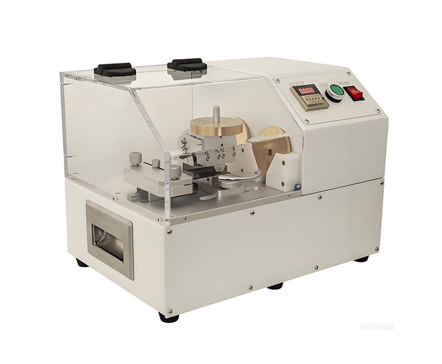
Mechanical cycling is the only way to reach the wear state that produces resistance drift. Equipment: Three Wheel Tester for ICC Card Mechanical Reliability.
Design and Specification Rules That Extend Life
✓ Gold thickness is a temperature decision
A thin flash passes every room-temperature test and fails in a kiosk in the sun, because nickel diffusion and oxide growth follow an Arrhenius curve. Specify gold against the maximum surface temperature the card will see, not only against insertion count.
✓ Nickel is a barrier, not a base layer
Two to six micrometres of nickel prevents substrate diffusion. Below one to two micrometres the gold is decoration and the barrier has already failed before the card leaves the plant.
✓ Wipe distance matters more than contact force
A longer wipe sweeps oxide debris out of the contact spot with less plating damage. Increasing force without increasing wipe moves the failure from high resistance to wear-through.
✓ Intermittent is a distribution word
A card that reads on the second insertion has a resistance problem at one pad, not a firmware problem. Collect the distribution of resistance by pad and the pattern usually identifies the reader population and the duty cycle.
Reference Values for Contact Interface Assessment
Reference bands for ISO/IEC 7816 ID-1 contact and dual-interface cards. Actual limits depend on the reader population, the insertion count expected over card life, and the maximum surface temperature in service, and must be confirmed by cycling your own card in your own reader geometry.
Where Contact Resistance Decides the Product
The same wear and fretting logic applies wherever a spring contact meets a plated pad for the life of a product:
- Banking and healthcare cards used in ATMs and desktop readers with high insertion counts
- Transit cards read in ticket machines exposed to vibration and wide temperature swings
- SIM and payment modules in phones and wearables, where micro-motion is continuous
- Dual-interface cards where the contact plate is also the mechanical interface to the antenna bridge
- Card readers in kiosks, where a single worn beam position damages an entire card population
Frequently Asked Questions
Does cleaning a returned card fix it?
Sometimes for a short time. A solvent removes the plasticiser and fingerprint film, but it does not restore gold that has worn through, and it also removes whatever lubrication the reader relied on. If nickel oxide is exposed in the scar, the card will fail again within weeks.
Why do cards fail in one reader type only?
Because the reader defines the force, the wipe and the parked position. A reader with low force and a short wipe will report high resistance on cards that another reader still accepts, and a reader with high force will wear plating that another reader never touches.
Is a very low contact resistance a problem?
Not electrically. The practical risk is measurement error: readings below ten milliohms usually indicate a two-wire measurement with probe resistance included, or a shorted test fixture, rather than an unusually good card.
Next Step
More equipment in this range is listed on the ZOWINDA CardMachine product page, and related application notes appear in our Industry News section.
Related reading:
- Electrochemical Migration at the Module Edge: Bias, Moisture and Ionic Cleanliness
- Booklet Spine Adhesive: Why Flexibility Beats Peel Strength
- Dual-Interface Bridge: Making the Contact and Contactless Paths Agree
- Isotropic Conductive Adhesive Cure: The Three-Variable Window Behind Module Opens
- Inlay-to-Body Registration: The Tolerance Chain Behind a Working Card
Ready to boost your production efficiency?
Contact us for a tailored solution and quotation on inlay production, card testing and personalisation equipment.
Email: info@zowinda.com
WhatsApp: +86 186 2085 0485
 Booklet Spine Adhesive: Why Fl
 Contact Plate Life: Wear, Fret
 Electrochemical Migration at t
 Laser Marking on Card Faces: C
Please contact us with your request
We are ready to answer your questions.