
Dual-Interface Bridge: Making the Contact and Contactless Paths Agree
Smart Card Manufacturing Notes
Dual-Interface Bridge: Making the Contact and Contactless Paths Agree
Published: November 16, 2026 | ZOWINDA Application Engineering
A dual-interface card carries two ways in and one chip behind them. The contact plate sits on the surface, the antenna is buried in the body, and a small tail of lead frame called the bridge connects the two. Almost everything difficult about dual-interface production happens in the few millimetres around that bridge, and almost every quality argument about dual-interface cards is really an argument about an assembly tolerance nobody wrote down.
What the Bridge Actually Is
On a contact-only card the module is a lead frame with six or eight contact pads on top and a chip bonded underneath, and the only external connection is the reader. On a contactless card the chip connects to an antenna through two pads. A dual-interface module combines both: the contact plate keeps its ISO 7816 pad layout, the chip behind it drives a radio front end, and two pads on the back of the module, usually designated LA and LB, connect down to the antenna ends buried in the card body. The bridge is that connection, and it is made at implanting time, not at module manufacturing time.
This is why the process sequence dominates the failure population. The cavity is milled to a depth that will leave the module flush, an adhesive or anisotropic film is placed, the module is inserted and cured, and only then is the bridge electrically continuous. If the antenna pads in the body are a tenth of a millimetre off, or the module tail lands on the pad edge rather than in its centre, the joint is marginal in a way that no visual inspection at the implant station will see. The card passes a functional test because the contact is good, ships, and comes back four months later with a contactless failure.
Electrically the bridge is also where two very different domains meet. The contact path is a direct galvanic connection, exposed to whatever a reader slot can deliver, including electrostatic discharge from a human hand. The contactless path is a tuned resonant circuit at 13.56 megahertz, where a few picofarads of stray capacitance at the bridge changes the resonance of the whole antenna. That is why the same card can pass contact testing and fail radio frequency testing: nothing is broken, the joint simply added capacitance. Fixture capacitance during test makes this worse, because a tester that grips the contact plate loads the circuit differently from an antenna in free space.
The mechanical side is equally specific. The bridge sits in the deepest part of the cavity, at the end of a tail that has to bend from the module plane down to the antenna plane, and it is surrounded by cured adhesive that is stiffer than the card body. When the card is bent, that transition is a stress riser: the adhesive holds the module rigid while the body flexes, and the tail takes the difference. A joint that measures a few milliohms on the line can lift after a thousand bend cycles, and the failure mode is an intermittent card rather than a dead one, which is the most expensive kind to diagnose in the field.
Inserting a Module Without Breaking the Bridge
- Fix the antenna pads as the datum, not the card edge. Cavity position must be derived from the antenna pad coordinates in the body, because the bridge lands on those pads. Cards are trimmed and printed to a card edge tolerance that is looser than the bridge needs, so using the edge as a datum stacks two tolerances where one will do.
- Write down the tolerance stack before buying equipment. Cavity position, cavity depth, module dimension, antenna pad position and adhesive spread each contribute. Add them and compare with the pad width. If the sum is larger than half the pad width, the process relies on luck, not on capability.
- Control adhesive volume by weight, not by eye. The bond line in a well-controlled dual-interface implant is fifteen to thirty micrometres. Slightly too much adhesive wicks over the antenna pad and insulates the bridge; slightly too little leaves voids that grow under thermal cycling. Dispense weight per cavity is the only variable that predicts both.
- Verify cure by resistance distribution, not by oven readout. An oven reaching its set point does not mean the adhesive under a module reached cure temperature. Plot contact resistance across a batch; a long tail on the distribution is under-cure, and under-cure is what produces field opens in hot climates.
- Test both interfaces after implanting and again after personalisation. Personalisation applies heat, pressure and electrical contact to the plate. A card that passed implant test can fail after personalisation because the plate was disturbed or the bridge was stressed. Two test points, both interfaces, every card.
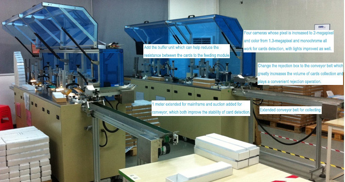
Implanting sets the bridge: cavity depth, adhesive volume and module position all move the joint. Equipment: Automatic Milling and Implanting Machine for Smart Card Modules.
Rules That Keep the Bridge Honest
✓ The bridge is a mechanical joint first
It survives or fails on flexure long before it fails on current. Qualify it with bending and torsion cycles followed by resistance measurement, not with a single functional pass.
✓ Never trust a one-interface test
A card that reads on contact proves the chip works. It says nothing about the antenna, the bridge or the resonant circuit. Dual-interface quality needs contact, radio frequency and resonance measured on the same card.
✓ Watch the ferrite under the bridge
Where a ferrite sheet stiffens the area around the antenna pads, the bridge sits on a brittle substrate. A cracked ferrite raises losses and detunes the antenna without breaking any electrical connection, so the card tests alive and reads short.
✓ Design the ESD path deliberately
The contact plate is the entry point for discharge during handling and personalisation. Add the discharge protection at the chip, and treat every contact-side test station as an ESD-controlled area, because a damaged input can present as a radio frequency fault.
Reference Values for Dual-Interface Assembly
Typical reference bands for a standard 0.76 millimetre dual-interface card with an etched or printed antenna. Values move with antenna design, ferrite construction, module supplier and card body material, so confirm them on first articles before setting process limits.
Where the Bridge Question Applies
The same joint appears wherever a surface contact has to reach a buried conductor inside a laminated body:
- Banking and transit cards required to work on both contact and contactless readers
- Government identity cards that combine a contact chip with a vicinity interface
- Healthcare and campus cards with a contact plate for legacy terminals
- Hybrid SIM formats where the same die serves both a slot and a radio path
- Any card where a module is implanted after lamination, which is most dual-interface production
Frequently Asked Questions
Can a card with a failed bridge be reworked?
Practically no. Removing a cured module from a milled cavity destroys the cavity wall and usually the antenna pads with it, and the body has already been through lamination. Rework of dual-interface cards at module level costs more than the card and adds a hidden population of previously heated bodies. Scrap and record it.
Why does a card pass contact testing and fail radio frequency testing?
Three common causes, in order of frequency: the bridge never made a reliable joint, the antenna was detuned by the implant or by the body, or the ferrite under the antenna cracked during implanting. Contact testing exercises none of these, which is why both interfaces have to be measured on every unit.
Does the contact plate have to be grounded to the antenna?
There is no universal requirement, but the design must decide deliberately. Some designs tie the plate to a chip ground for ESD reasons, which introduces a path between the two domains and can shift resonance. Whatever the choice, it belongs in the module specification, not in a supplier default discovered during qualification.
Next Step
More equipment in this range is listed on the ZOWINDA CardMachine product page, and related application notes appear in our Industry News section.
Related reading:
- Laser Cutting or Die Cutting: How the Cavity Edge Decides Card Reliability
- Key Injection and Audit Trail: The Part of Personalisation That Gets Audited
- Automatic Milling and Implanting Machine for Smart Card Modules
- Gold Bump Flip-Chip or Wire Bonding: Choosing the Module Interconnect
Ready to boost your production efficiency?
Contact us for a tailored solution and quotation on inlay production, card testing and personalisation equipment.
Email: info@zowinda.com
WhatsApp: +86 186 2085 0485
 Key Injection and Audit Trail:
 Dual-Interface Bridge: Making
 Laser Cutting or Die Cutting:
 Reel-to-Reel or Sheet-to-Sheet
Please contact us with your request
We are ready to answer your questions.