
Electrochemical Migration at the Module Edge: Bias, Moisture and Ionic Cleanliness
Smart Card Manufacturing Notes
Electrochemical Migration at the Module Edge: Bias, Moisture and Ionic Cleanliness
Published: November 19, 2026 | ZOWINDA Application Engineering
The failure that ends a card programme is rarely a wrong antenna. It is a card that passed final test, shipped, and then reads intermittently eighteen months later in one market only, recovers when it is warm and dry, and cannot be reproduced on any bench in the factory. That signature, reversible and humidity-linked and slowly worsening, is the fingerprint of electrochemical migration at the module edge, and it is a cleanliness problem far more often than a design problem.
Why the Module Edge Is the Weak Point
In a contactless or dual-interface card the module edge is where three dissimilar materials meet inside a narrow gap: the lead frame or antenna pad, the encapsulant or underfill, and the card body. Conductor spacing across that gap is typically one hundred to three hundred micrometres. The bias across it can be several volts on the contact side of a dual-interface card, or a small standing offset on the antenna side where a rectifier and the reader field interact. Any ionic film that bridges the gap is an electrolyte; with a sustained DC bias, metal dissolves at the anode and plates back as a dendritic deposit at the cathode. The dendrite crosses the gap over weeks rather than seconds, which is exactly why the card passes at the end of the line and fails in service.
Three conditions have to be present at the same time for the mechanism to run: an ionic transport medium, a continuous bias, and a physical path. Remove any one and it stops. This is why the problem looks random and why a clean, dry test on a returned card proves nothing at all. Pure water at high relative humidity is a poor conductor; water plus ten to twenty micrograms per square centimetre of ionic residue is a good one, because salts deliquesce and form a continuous film at sixty to eighty per cent relative humidity, well below saturation. The moisture is the variable that the factory never has and the field always has.
The ionic residue has a short list of origins, and they are worth checking in this order. Flux residue from module soldering or reflow, where the activator rather than the rosin is the problem. Plating bath salts trapped in a porous or burnt deposit. Amine and acid residues left by adhesives and encapsulants that cure incompletely. Chlorine from a PVC card body, which is released as hydrogen chloride at lamination temperature and stays in the stack. Sulfur from vulcanised rubber rollers, from EPDM seals and from some wallet materials. And handling, where a fingerprint is a mixture of sodium chloride and fatty acids delivered directly to the pad.
The path is usually the cavity wall. A die-cut cavity has a rougher, more permeable edge than a milled one, and a laser-cut cavity leaves a carbonised zone that can delaminate under thermal cycling. If the encapsulant does not wet the wall, the interface becomes a capillary, and a capillary is a permanent route for moisture into the one region where two conductors are closest together. Seal the lid and ignore the wall and the mechanism simply relocates.
How to Qualify for Migration Instead of for Function
- Establish a dry insulation baseline, per pad and pad to antenna. Measure insulation resistance between adjacent contacts and between contact and antenna on dry cards, at a defined test voltage, and record the distribution rather than one value. Without a dry baseline you cannot tell reversible migration from permanent corrosion later.
- Run a biased humidity test, not unbiased damp heat. Forty degrees Celsius, ninety to ninety-three per cent relative humidity, bias at the highest DC voltage the product will see in service, five hundred to one thousand hours. Read insulation resistance at intervals without opening the chamber, because opening it resets the very film you are trying to grow.
- Add a dry and re-humidify step to separate the mechanisms. If resistance recovers after twenty-four hours at fifty degrees Celsius and collapses again on re-exposure, the failure is ionic and reversible. If it does not recover, the dendrite or the corroded pad is permanent and the card is scrap.
- Section the module edge when resistance falls. Ion chromatography on an extract of the module region gives chloride, sulfate, bromide and weak organic acid levels. A cross-section of the cavity wall shows delamination, voids and the dendrite itself. Both are needed: the chemistry tells you the source, the section tells you the path.
- Fix the source and re-qualify with the same test. A changed flux, a plasma step before encapsulation or a new body grade is a hypothesis, not a fix, until the same biased humidity test produces the same or better numbers. Keep the extract conductivity and chromatography results with the lot record.
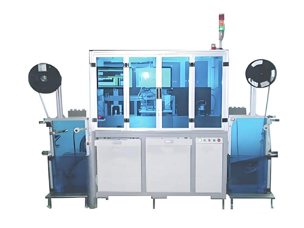
Module-level electrical testing screens function, not ionic cleanliness; the two are not the same acceptance criterion. Equipment: Automatic Module Testing Machine for Smart Card IC Modules.
Process Controls That Actually Remove the Mechanism
✓ Cleanliness is a specification, not a habit
Set an extract conductivity limit and an ion chromatography limit on the module before encapsulation, and measure it on samples from every plating and reflow batch. A number in a specification is auditable; good practice on the floor is not.
✓ Seal the wall, not just the lid
Plasma activation before encapsulation improves wetting at the cavity wall, and dye penetration after cure shows whether the seal is continuous. The wall is where the conductors are closest, so it is where the seal has to be best.
✓ Keep chlorine and sulfur out of the body
A PVC body is a chloride reservoir sitting millimetres from the gap. Low-chloride grades, PET-G and polycarbonate reduce the reservoir, and sulfur-free rubber removes the other common source.
✓ Give the gap distance and a dam
Wider spacing at the cavity wall and a solder mask dam between adjacent conductors cost almost nothing at design stage and buy real margin. A dendrite has to travel the whole gap to fail the card.
Reference Values for a Migration Assessment
Reference bands for 13.56 MHz contactless and dual-interface cards with a milled or die-cut module cavity. Actual thresholds depend on conductor geometry, encapsulant chemistry, body material and the DC bias present in your application, and must be confirmed by testing your own product against your own acceptance limits.
Where the Mechanism Applies
The same three-condition logic applies to any sealed electronic assembly that carries a DC bias across a narrow gap:
- Dual-interface banking and transit cards, where the contact side supplies a standing DC bias
- ePassport data page modules, where the booklet is carried for ten years in humid climates
- Plug-in SIM and payment modules handled daily with contaminated fingers
- NFC tags and labels on laundry, medical packaging and outdoor assets
- Cards returned from tropical markets where the failure never reproduces in a European laboratory
Frequently Asked Questions
Does a conformal coating solve it?
A coating blocks the water path and slows the mechanism, but it does not remove the ionic residue underneath. If residue is trapped and then humidified through a pinhole, the failure moves rather than disappears. Clean first, then coat, and verify the coating has no porosity at the cavity wall.
Why does only one market report failures?
Migration is driven by humidity, duty cycle and the DC bias the local readers apply. A market with higher humidity, more time parked in a reader, or a different reader population can fail a card that passes everywhere else. That is a data point about the mechanism, not about card quality variation.
Can the antenna side fail the same way?
Less often, because the RF field is alternating and does not sustain a net DC bias. It becomes plausible on dual-interface cards where a rectifier, a standing offset or a damaged bridge creates a DC path between antenna and ground. Once that path exists, the antenna side behaves like the contact side.
Next Step
More equipment in this range is listed on the ZOWINDA CardMachine product page, and related application notes appear in our Industry News section.
Related reading:
- Contact Plate Life: Wear, Fretting and Contact Resistance Drift
- Booklet Spine Adhesive: Why Flexibility Beats Peel Strength
- Laser Cutting or Die Cutting: How the Cavity Edge Decides Card Reliability
- Card Body Thermal Budget: PVC, PET-G and Polycarbonate Lamination Windows
- Dual-Interface Bridge: Making the Contact and Contactless Paths Agree
Ready to boost your production efficiency?
Contact us for a tailored solution and quotation on inlay production, card testing and personalisation equipment.
Email: info@zowinda.com
WhatsApp: +86 186 2085 0485
 Booklet Spine Adhesive: Why Fl
 Contact Plate Life: Wear, Fret
 Electrochemical Migration at t
 Laser Marking on Card Faces: C
Please contact us with your request
We are ready to answer your questions.