
Inlay-to-Body Registration: The Tolerance Chain Behind a Working Card
Smart Card Manufacturing Notes
Inlay-to-Body Registration: The Tolerance Chain Behind a Working Card
Published: November 18, 2026 | ZOWINDA Application Engineering
Ask three people where the registration specification on a smart card comes from and you will get three answers: the printer will quote a print registration figure, the punch operator will quote a cavity position tolerance, and the implant engineer will quote a placement repeatability. All three are correct and none of them is the specification, because a card reads or fails on the relative position of two features that are made by different processes, on different machines, at different times. Registration is a chain, and a chain is only as good as the way its links combine.
Two Datums Live on Every Card
Every card carries a print datum and an electrical datum, and they are not the same coordinate system. The print datum is the card edge or a printed registration mark, and it is what the visual inspection station checks when it confirms that the logo, the foil patch and the guilloche line up. The electrical datum is the antenna pad or the module cavity, and it is what decides whether the chip actually connects. On a contactless card the antenna is printed on a web with its own registration tolerance, then laminated, then often punched, and the cavity is positioned relative to print marks rather than relative to the antenna pads, because that is what the punch can see.
The consequence is a systematic error that nobody owns. If the antenna print sits fifty micrometres to the left of the artwork centre and the cavity is punched perfectly to the print mark, every card in the lot carries the module fifty micrometres off the pad centre. That error does not appear as a reject on the punch, it appears later as a weak or open interconnect at the implant or flip-chip station, and it will be blamed on that station. Measuring only one datum guarantees this outcome, because each process reports itself as capable while the pair drifts.
The physical requirement is blunt: the module pad and the antenna pad have to overlap across the whole of the joint, with enough margin that adhesive cure shrinkage, thermal cycling and bending do not open it. A conductive adhesive joint needs an overlap of at least a tenth to two tenths of a millimetre on each side after worst-case misalignment; a wire-embedded connection needs the wire end to land inside the pad zone with similar margin. That overlap, not the individual machine tolerance, is the number to design and to audit.
This is also why lamination belongs in the chain rather than outside it. PVC and PET-G shrink during lamination, and the shrink is anisotropic: it is larger along the machine direction than across it, and it scales with sheet size and with the thermal profile. A sheet can come out of the press with a card pattern that is dimensionally correct at the edges and displaced in the centre, which means registration error is a function of position on the sheet. Any sampling plan that inspects only edge cards will under-report it, and any offset compensation derived from edge cards will over-correct the middle.
Building the Chain Instead of Guessing It
- Draw both datum systems and name the owner of each. Put the print datum and the electrical datum on one drawing with the processes that establish them. If a feature is controlled by two processes and specified by neither, that is where the error will hide.
- Collect measured spread per contributor, not datasheet maxima. For each link, take at least thirty consecutive parts and record mean and standard deviation: antenna print registration, sheet cutting, lamination shrink along both axes, cavity position, collation offset, implant placement. Datasheet limits describe a machine, standard deviations describe your line.
- Separate the constant offset from the scatter. A mean shift can be compensated once by nudging the cavity file or the print artwork. Scatter cannot be compensated, only reduced or absorbed by design margin. Mixing the two into a single plus or minus figure is the most common analytical mistake in this area.
- Combine the links correctly before allocating margin. Independent contributors combine as the root sum of squares, not by simple addition, but contributors on the same sheet and in the same direction are correlated and behave closer to linear addition. Design the pad overlap for three standard deviations of the measured combined distribution, then verify by measurement rather than trusting the arithmetic.
- Audit the finished card, per position on the sheet. Cross-section or X-ray a grid of cards from one sheet and record module-to-pad offset as a map. A stable map with a centre-to-edge gradient means lamination shrink dominates; a random map means handling or placement dominates. The fix is completely different in each case.

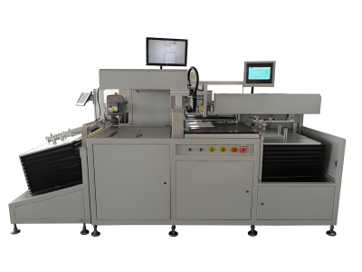
Registration is fixed at the collation and bonding stage, where two separately made patterns are brought together. Equipment: Sheet Positioning and Bonding Machine for Smart Card Production.
Rules That Keep the Two Datums Together
✓ Pad overlap is the only registration specification that pays
Print registration is a customer-visible figure and it matters, but the card fails electrically on pad overlap. Specify overlap after worst-case shift, then derive the allowable machine tolerances backwards from it.
✓ Lamination shrink is a direction, not a scalar
Machine-direction shrink differs from cross-direction shrink, and the difference rotates the error field across the sheet. Compensate the artwork in two axes, and re-check the compensation whenever the laminator recipe changes.
✓ One datum per process, joined by a measured bridge
Let the punch work to print marks because that is what it can see, but measure the antenna-to-print relationship on every antenna lot and feed it back as a known offset. The bridge is a measurement, not an assumption.
✓ A vision system proves print, not connection
A camera that confirms the print is on centre says nothing about whether the bump sits on the pad. Add an electrical or X-ray check at the joint, at a frequency that matches the cost of a field return.
Reference Values for the Registration Chain
Typical reference bands for 13.56 MHz dual-interface and contactless cards built from printed inlays in 0.76 to 0.84 millimetre bodies. Real limits depend on antenna pitch, pad geometry, adhesive system, sheet size and laminator profile, and must be established from your own measured distributions.
Where the Registration Chain Applies
The same chain analysis applies wherever two independently made patterns have to meet inside one product:
- Dual-interface bank and ID cards where the contact plate, the bridge and the antenna must agree
- Contactless inlays with strap or flip-chip interconnects on a printed antenna web
- RFID labels where antenna registration and die-cut registration decide the read zone
- Cards with windows, transparent areas or special shapes where the punch defines the outline
- Electronic passport inlays where the antenna has to clear the spine and the data page edge
Frequently Asked Questions
Can we simplify by punching the cavity to the antenna instead of the print?
You can choose either datum, but not both. Punching to the antenna improves the electrical joint and degrades print registration, because the print was registered to the card edge. Most production lines keep the print datum for the punch and carry a measured antenna-to-print offset, which keeps both numbers visible.
Why do all the cards from one sheet fail together?
Because the contributors inside one sheet are correlated: one lamination cycle, one shrink field, one punch stroke, one collation pass. The sheet behaves as a single sample of the process, not as hundreds of independent ones. That is also why a sample of one card per sheet is a weak audit.
Is a placement repeatability of plus or minus 0.05 millimetres good enough?
It is good, and it may still be irrelevant. If the cavity is offset by 0.15 millimetres because the antenna print drifted, a precise placer puts the module precisely in the wrong place. Precision downstream cannot recover accuracy lost upstream, which is why the chain has to be measured end to end.
Next Step
More equipment in this range is listed on the ZOWINDA CardMachine product page, and related application notes appear in our Industry News section.
Related reading:
- Card Face Printing and Read Range: Where Ink and Overlay Sit in the Stack
- Laser Marking on Card Faces: Contrast, Depth and Surface Integrity
- Laser Cutting or Die Cutting: How the Cavity Edge Decides Card Reliability
- High-Speed RFID Card Production Inlay Sheet Manufacturing Line
- Gold Bump Flip-Chip or Wire Bonding: Choosing the Module Interconnect
Ready to boost your production efficiency?
Contact us for a tailored solution and quotation on inlay production, card testing and personalisation equipment.
Email: info@zowinda.com
WhatsApp: +86 186 2085 0485
 Laser Marking on Card Faces: C
 Inlay-to-Body Registration: Th
 Card Face Printing and Read Ra
 Key Injection and Audit Trail:
Please contact us with your request
We are ready to answer your questions.