
Gold Bump Flip-Chip or Wire Bonding: Choosing the Module Interconnect
Smart Card Manufacturing Notes
Gold Bump Flip-Chip or Wire Bonding: Choosing the Module Interconnect
Published: November 14, 2026 | ZOWINDA Application Engineering
Every contactless card contains one decision made once and repeated millions of times: how the silicon gets connected to the antenna. Wire bonding and gold bump flip-chip both work, both ship in billions of units, and neither is simply better. The right answer depends on cavity depth, cycle time and who owns the failure analysis when a joint goes wrong.
Two Geometries, Two Failure Populations
Wire bonding is the older and more flexible process. The die sits face up, connections rise from the die pads in aluminium wedge or gold ball loops and come down onto the antenna or lead frame pads. Because the loop arches above the die surface, the finished assembly is taller: a wire-bonded module typically stands 200 to 300 micrometres proud of the die face, against roughly 60 to 100 micrometres for a bump-flip-chip joint. That height difference decides where the technology can live. Inlays destined for milled cavities in standard 0.84 millimetre cards favour the low profile of flip-chip; thicker formats, dual-interface modules with their own carriers, and prototype work favour the simplicity of wire.
Flip-chip reverses the geometry. The die carries gold bumps formed on the wafer, is flipped face down, and the bumps land directly onto antenna pads through an isotropic conductive adhesive or, less commonly in cards, solder. Alignment is optical and self-centring to a degree, placement is fast, and there is no loop to catch on downstream tooling. The cost of that elegance sits upstream: bumped wafers are a purchased item with lead time and a defined bump layout, so the interconnect is decided at wafer level, months before the card is laminated.
The failure populations differ in kind, not just in rate. A wire bond fails visibly and locally: a lifted ball, a broken loop at the heel, a squashed wedge. Optical inspection catches most of them before the module leaves the line. A flip-chip joint built on conductive adhesive fails electrically and invisibly: the joint conducts at the line and drifts in the field when the cure was incomplete, which is why electrical screening and thermal cycling carry more weight in flip-chip qualification than in wire qualification.
Throughput also splits the decision. A modern ball bonder places thousands of wires per hour but pays that rate once per pad pair; a flip-chip placer pays once per die, and a die has all its interconnects made in a single placement. For standard contactless inlays with two to eight pads, flip-chip wins on cycle time at volume. For engineering builds, mixed pad layouts and low volume, wire avoids the bump mask economics entirely.
How to Decide Without Guessing
- Start from the cavity, not from the die. Measure the depth the finished module may occupy after lamination and subtract the card body tolerance. If the budget is under 150 micrometres above the die face, wire bonding is out before any other criterion is discussed.
- Count pads and volume honestly. Two pads on a payment inlay at ten million units per year is a flip-chip economics argument. Forty pads on a dual-interface module at fifty thousand units is a wire argument. Between the extremes, price both routes including wafer bumping and set-up.
- Qualify the joint for its own failure mode. For wire, qualify with pull and shear plus optical heel inspection. For adhesive flip-chip, qualify with contact resistance distribution and thermal cycling, because the passing unit at the line is not proof the cure was complete.
- Check the downstream stack height together. The interconnect height feeds cavity depth, which feeds ferrite thickness and antenna keep-out on dual-interface cards. Choose the interconnect with the mechanical stack on the table, not in isolation.
- Agree the electrical test point before production. Whichever route is chosen, define what the tester measures on every module and what it infers. A wire bond can be optically verified; a flip-chip joint mostly cannot, so the electrical test has to carry the guarantee.

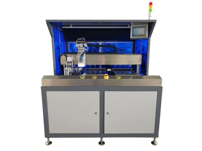
Die placement is common to both routes; the interconnect above the die decides the cavity budget. Equipment: Auto COB Pick and Placer Machine.
Where Each Route Earns Its Place
✓ Flip-chip for height and rate
Low profile above the die and one placement per die make it the default for high volume contactless inlays and any cavity-limited stack.
✓ Wire for flexibility and prototypes
No bumped wafer needed, any pad layout bondable, and loop height adjustable in parameters. Engineering builds and mixed formats run on wire without wafer commitments.
✓ Match inspection to failure mode
Wire bonds reward optical inspection; adhesive flip-chip joints reward resistance statistics and cycling. Budget inspection where the failure mode actually lives.
✓ Treat bumps as a supply decision
Gold bump flip-chip locks the die to a bump layout and a wafer supplier. For long-lived products that is an advantage in consistency; for volatile designs it is a constraint.
Reference Values for Both Interconnects
Typical reference ranges for smart card module assembly. Actual values depend on die size, pad layout, adhesive system and the cavity budget of the card body, and should be confirmed on first articles.
Where the Choice Applies
The same decision framework covers any assembly where a die is connected to a printed or etched conductor:
- Contactless and dual-interface inlay production at volume
- ePassport and ID-1 module assembly in milled polycarbonate cavities
- Chip-on-label and NFC tag assemblies with tight height budgets
- Engineering and low volume builds where bumped wafers are uneconomic
- Any programme comparing cycle time against wafer supply commitments
Frequently Asked Questions
Is gold bump flip-chip always more reliable than wire bonding?
No. It has a lower profile and fewer handling loop failures, but the joint is adhesive based and its dominant failure mode, resistance drift from incomplete cure, has no optical signature. Wire bonding fails visibly and is easier to screen. Reliability follows the qualification effort put on the right failure mode, not the technology label.
Why do dual-interface cards often keep wire bonding?
Because the module carrier sits in a dedicated milled cavity with more height allowance, the loop is less of a constraint, and dual-interface designs change more often, which suits the flexibility of wire over the fixed geometry of bumped wafers.
Can a line run both interconnects?
Yes, and many do: flip-chip placers for volume inlay products, a bonder for specials and rework. The disciplines differ enough, particularly in inspection and cure control, that treating them as one process with two recipes is a common source of escapes.
Next Step
More equipment in this range is listed on the ZOWINDA CardMachine product page, and related application notes appear in our Industry News section.
Related reading:
- Card Body Thermal Budget: PVC, PET-G and Polycarbonate Lamination Windows
- Reel-to-Reel or Sheet-to-Sheet: Matching Inlay Architecture to Volume
- Automatic IC Module Testing Machine for Smart Card Production
- Isotropic Conductive Adhesive Cure: The Three-Variable Window Behind Module Opens
Ready to boost your production efficiency?
Contact us for a tailored solution and quotation on inlay production, card testing and personalisation equipment.
Email: info@zowinda.com
WhatsApp: +86 186 2085 0485
 Reel-to-Reel or Sheet-to-Sheet
 Gold Bump Flip-Chip or Wire Bo
 Card Body Thermal Budget: PVC,
 Isotropic Conductive Adhesive
Please contact us with your request
We are ready to answer your questions.