
Printed Antenna Tolerance: Which Dimension Actually Moves Resonance
Smart Card Manufacturing Notes
Printed Antenna Tolerance: Which Dimension Actually Moves Resonance
Published: November 13, 2026 | ZOWINDA Application Engineering
An inlay antenna is designed at one frequency and produced at another. The gap between the two is usually blamed on the tolerance that is easiest to measure. This note ranks the real contributors to resonance shift on 13.56 MHz inlays and shows where a millimetre of conductor length is worth more than a tightened line width.
The Resonance Equation Is Simple; Its Inputs Are Not
Every HF inlay is a parallel resonant circuit. Frequency follows f = 1 / (2 x pi x square root of L times C), where C is the chip input capacitance plus the parasitic capacitance of the coil against its own environment. Because both terms sit under a square root, a one percent error in inductance moves frequency by about half a percent, and the same holds for capacitance. At 13.56 MHz that half percent is roughly 68 kHz, which is a useful unit to keep in mind for the rest of this note.
Inductance itself is set by four things, in descending order of influence: total conductor length around the spiral, the mutual coupling between adjacent turns, the corner and bridge geometry, and only then the trace width. Width is the parameter most often specified on a drawing and least often responsible for a detuned batch. Doubling the trace width on a typical four-turn coil changes inductance by a fraction of a percent, while it changes series resistance and therefore Q by a factor close to two.
Capacitance is where production reality enters. The antenna is never measured in air. A bare inlay carries a 50 micrometre PET substrate with a relative permittivity near 3.2, an adhesive layer, and then whatever card body it is laminated into: PVC near 3.0, PET-G near 3.3, polycarbonate near 2.9. Effective permittivity around the conductor climbs from 1 in air to the 2.5 to 3.5 range once the stack is closed, parasitic capacitance rises with it, and resonance falls. A PVC body typically pulls a bare inlay down by 0.4 to 0.9 MHz, and that shift is a property of the design stack, not of the printer.
The practical ranking for a converter is therefore: conductor length and geometry first, dielectric stack second, chip input capacitance spread third, trace width fourth, turn-to-turn gap fifth. Any tolerance chart that puts width at the top is a chart that measures what is convenient rather than what moves the number. The consequence is straightforward. If you have budget to tighten one thing, tighten the length, and hold the dielectric stack constant by qualifying substrate and adhesive lots against a reference coupon.
A Measurement Sequence That Separates Design Offset from Process Scatter
- Budget the circuit before the artwork is released. Take the chip input capacitance from the datasheet, add the parasitic estimate for your stack, and compute the conductor length that lands on 13.56 MHz after dielectric loading. Write the target bare-inlay frequency above nominal, not at nominal, because the card body will pull it down later.
- Measure bare inlay resonance on a coupon from every sheet. One coupon at the sheet edge, measured dry and unloaded, gives you the printing process signature. Record the value against sheet number rather than against time, since drift tracks tooling and ink lot more closely than the clock.
- Measure again after the first lamination. The difference between the two readings is dielectric loading plus adhesive flow. If this difference varies by more than 0.2 MHz across a lot, the problem is in the laminating stack, not in the printing.
- Split the data into offset and scatter. Offset is a constant you can design out by shifting artwork length. Scatter is random and can only be reduced by process control. Averaging a batch tells you the offset; the standard deviation tells you whether the line is capable.
- Feed corrections back as length, not as width. A two millimetre change on the outer turn of a typical HF coil moves resonance by roughly 0.15 MHz. Correct batches by trimming length or revising artwork. Correcting by narrowing traces buys frequency at the cost of Q, which is a bad trade because read range depends on Q as much as on tuning.

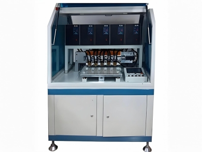
Inlay sheets leave the line with a measurable resonance already fixed by geometry and substrate. Equipment: High-Speed RFID Inlay Sheet Manufacturing Line.
Where the Yield Is Actually Recoverable
✓ Design offset, not tighter tolerance
Pre-compensate the artwork for the measured dielectric pull of your specific card body. A fixed offset costs nothing per unit, while tightening registration tolerance costs tooling time on every run.
✓ Length trim per batch
Treat antenna length as an adjustable parameter with a known sensitivity in kHz per millimetre. Two or three trims per year are usually enough to keep a mature product centred.
✓ Coupon discipline beats sampling plans
A coupon on every sheet detects a tooling drift within one sheet. Sampling three sheets per shift detects it after the non-conforming material has already been laminated.
✓ Width belongs to Q, not to frequency
Specify trace width to control resistance and Q at 13.56 MHz. Expect roughly 0.02 MHz of frequency movement per 0.05 mm of width change, which is inside the noise of most processes.
Reference Values and Tolerances
Typical reference values for HF inlays on a PET substrate. Actual windows depend on chip capacitance, card body material and reader field strength, and should be confirmed on your own stack before being written into a specification.
Where These Numbers Apply
The analysis holds for any inductively coupled product where the coil is printed or etched and then buried in a dielectric:
- Contactless payment and transit cards in PVC, PET-G or polycarbonate bodies
- Dual-interface cards, where the metal module adds a further detuning term
- NFC tags and labels where the antenna is printed on paper or thin film
- Inlay sheets produced as a panel and later cut, where edge coupons represent the panel
- Any programme where read range complaints arrive after lamination rather than at incoming inspection
Frequently Asked Questions
Does a narrower trace lower the resonant frequency?
Almost the opposite. Narrowing a trace reduces mutual coupling between turns slightly, which lowers inductance marginally and pushes resonance up by a few tens of kHz. What changes decisively is series resistance, which rises and drags Q down. A card that reads short after a width reduction is usually losing Q, not detuning.
Why does an inlay read perfectly on the bench and poorly inside the card?
Because the bench measurement is unloaded. Lamination adds dielectric material around the conductor, raises parasitic capacitance and pulls resonance down by 0.4 to 0.9 MHz depending on body material. If the design was centred on 13.56 MHz bare, it will sit low in the finished card, outside the reader tolerance band.
How often should resonance be re-measured?
One coupon per sheet for printing, plus one finished card per lamination batch. Trend the readings rather than judging them individually, and set an alarm at three sigma of the historical distribution. A single out-of-window reading is information; a trend is a decision.
Next Step
More equipment in this range is listed on the ZOWINDA CardMachine product page, and related application notes appear in our Industry News section.
Related reading:
- Dual-Interface Ferrite: Why Sheet Thickness Beats Permeability on the Datasheet
- Isotropic Conductive Adhesive Cure: The Three-Variable Window Behind Module Opens
- Automatic Frequency Test Machine for RFID and NFC Cards
- Contactless Card Read Range: Diagnosing Antenna Resonance and Detuning
Ready to boost your production efficiency?
Contact us for a tailored solution and quotation on inlay production, card testing and personalisation equipment.
Email: info@zowinda.com
WhatsApp: +86 186 2085 0485
 Isotropic Conductive Adhesive
 Dual-Interface Ferrite: Why Sh
 Printed Antenna Tolerance: Whi
 Contactless Card Test Programm
Please contact us with your request
We are ready to answer your questions.